


Chinese scientists adopt new technique to create faster microchips for AI devices

Chinese scientists replace traditional silicon with 2D materials in AI chips.
- Chinese scientists created new materials to replace silicon in AI chips.
- Researchers used 2D materials to create new ultra-thin chips.
- New chips will be smaller and have more computational power while utilizing less energy.
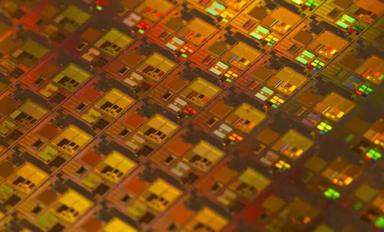
Chinese scientists have developed a new ultra-thin semiconductor material that is said to help create speedy and more energy-efficient microchips. These chips will power artificial intelligence applications on devices.
The new semiconductor material is only 0.7 nanometers thick. The fabrication method was developed by a team led by Zhang Guangyu of the Chinese Academy of Sciences and Liu Kaihui from Peking University, according to a report by South China Morning Post. The new chips are expected to boost power for on-device artificial intelligence applications.
Chinese scientists used 2D material to replace silicon for AI chips
The researchers have addressed a major hurdle in reducing the size of the traditional silicon chips. As electronic devices are shrinking in size, traditional computing chips hit their physical limits that affect their performance.
Also read: Biden funds virtual semiconductor modeling hub
The Chinese scientists worked on two-dimensional transition-metal dichalcogenides (TMDs) as a possible alternative to traditional silicon. The difference in thickness of the material is quite significant as TMD is 0.7 nanometers compared to 5 to 10 nanometers of silicon.
An additional benefit is that TMD-based chips consume less power, and their electron transport properties are better than those of silicon. This makes them a better choice for extremely scaled-down transistors for next-generation photonic and electronic chips.
Impure crystals are often created during traditional fabrication because atoms are assembled layer-by-layer on a substrate. For the sake of understanding, it can be said that the process is the same as building a wall with bricks, Kaihui told news agency Xinhua. He said,
“This is due to uncontrollable atomic arrangements in crystal growth and the accumulation of impurities and defects.”
A fingernail size chip will have more computing power
The team positioned the first layer of atoms on the substrate during the process, as is done in a traditional process. The difference was made by placing subsequent atoms between the crystal’s first layer and substrate.
The new technique is called “grow at interface,” which ensures that properties of structure of each individual crystal layer are perfectly dictated by the substrate below it. This also helps in preventing the accumulation of defects at one point and enhances structural precision.
Also read: US and EU utilize AI in search for alternatives in semiconductor manufacturing
According to the information on Peking University’s website, the study achieved a crystal layer formation rate of 50 layers per minute. The technique was able to create a maximum of 15,000 layers.
The university said that the atomic alignment in each layer is precisely managed and perfectly parallel to each other. The crystals created were made of materials that were of international standards, such as molybdenum disulfide, niobium disulfide, and a few others. All these materials were in accordance with global standards for integrated circuit materials, said the researchers.
Liu said that these 2D crystals, when used with other materials for transistors, have the ability to improve chip integration. The density of transistors can be substantially increased to boost computing power and that on a microchip the size of a fingernail.
Don’t just read crypto news. Understand it. Subscribe to our newsletter. It's free.
Disclaimer. The information provided is not trading advice. Cryptopolitan.com holds no liability for any investments made based on the information provided on this page. We strongly recommend independent research and/or consultation with a qualified professional before making any investment decisions.

Aamir Sheikh
Aamir is a tech journalist with nearly six years of experience in the crypto and tech industries. He graduated from MAJ University with an MBA in Finance and Marketing. He now works with Cryptopolitan, where he reports on the latest developments in the cryptocurrency markets and price prediictions.